RecommendMail Facebook LinkedIn
Quick, easy wafer-level PIC testing: a Jenoptik product innovation for a future growth market
Photonic integrated circuits (PICs) are the chips of the future. In late 2020, Jenoptik launched its UFO Probe® Card. Employing existing test equipment for microeletronics to make PIC wafer-level testing easy, quick, and affordable. For Jenoptik, this marks the entry into one of the most promising photonics markets.
PICs of various types are produced on wafers using the conventional methods and equipment available to established semiconductor manufacturers. The wafers are produced in a very similar way to the electronic components, but new challenges present themselves during final wafer-level testing, which, due to the additional optical tests, is still light years away from the testing throughput of the microelectronics industry. At present, the test equipment’s optical interfaces need to be realigned in the sub-micrometer range for each chip. Considering the sheer number of chips, this process is extremely time-intensive and may involve up to several hours for each wafer. In some cases, this may mean that just a few wafers can be measured per day.
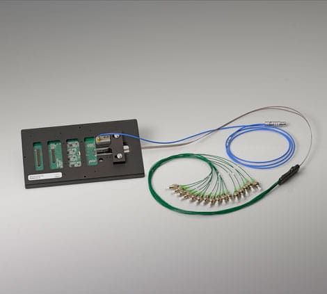
With the new Jenoptik solution, which is based on an optical concept that is insensitive to alignment tolerances, this additional testing time for a PIC wafer is reduced to just a few minutes, allowing wafers to be fully measur ed in a few hours. The new technology also enables parallel testing of several chips and can thus significantly reduce measuring times. The opto-electronic probe card can be integrated in commercially available wafer probers for microelectronics and easily adapted to a specific PIC layout and test setups.
For wafer inspection in semiconductor manufacturing, Jenoptik is a long standing supplier and partner to the semiconductor equipment industry and can draw on extensive process expertise. With the new UFO Probe® technology, Jenoptik is entering the market for PIC wafer-level testing in the semiconductor industry.
To help optimize, evolve, and market this technology, Jenoptik cooperates with probe card manufacturers and maintains close contact with end users. The new hybrid probe card, for example, combines electrical and optical inspections in a single solution. This allow multiple optical and electrical channels of a PIC to be tested in parallel, regardless of their arrangement, thus meeting the demand for opto-electronic tests for high-volume applications. The first series run was successfully measured with this new technology in late 2020.
PICs in optical transceivers transmit data using light instead of electrons. They enable energy savings and greater bandwidths at the same time, and are therefore used in conventional data transfer scenarios, such as in large data centers and data transmission cables, but also in gene sequencing and blood analysis, for example. Especially for IoT (Internet of Things) applications, PICs are expected to enjoy strong growth in the future due to their flexible chip design and excellent chip and performance characteristics. This is just beginning, because the basis for many new applications is the upcoming 5G network. According to the calculations provided by a market research institution, the total market for PICs is expected to rise from USD 4 billion in 2018 to more than USD 19 billion in 2024, thus growing by an average of more than 44 percent annually. This strong growth will be driven primarily by sensors, LiDAR, cell phones, and assistance systems for real-time responses in vehicles and production environments.